


![[Upcoming Webinar] Addressing the Wind Industry's €25 Billion Annual Wake Loss Problem](https://www.windesco.com/hubfs/Swarm%20webinar%20cover%20image.png)


Fraunhofer ISE streamlines use of epitaxial wafers in TOPCon solar cell manufacturing
Researchers at the German research institute have demonstrated that the so-called EpiWafers could be used directly for solar cell fabrication without needing a pre-gettering step. Their experiments provide a proof of principle* for epitaxially grown silicon wafers from German wafer manufacturer NexWafe GmbH.
Researchers at the German research institute have demonstrated that the so-called EpiWafers could be used directly for solar cell fabrication without needing a pre-gettering step. Their experiments provide a proof of principle* for epitaxially grown silicon wafers from German wafer manufacturer NexWafe GmbH.
A research group at Germany's Fraunhofer Institute for Solar Energy Systems (Fraunhofer ISE) has shown that in situ gettering during the application of asymmetric configuration of n-type and p-type tunnel oxide passivating contact (TOPCon) layers increases the material quality of n-type epitaxially grown silicon wafers.
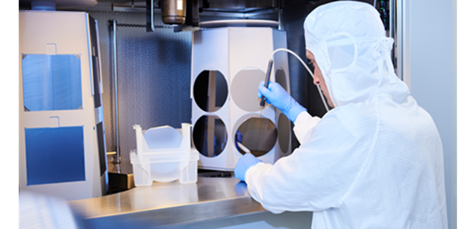
Gettering is a process widely used in the PV manufacturing industry during crystal growth to remove impurities and defects in wafers. Epitaxially grown wafers (EpiWafers) are fabricated in a direct gas-to-wafer process as a low-carbon material for solar cells.
“The key finding of our recently published work is that EpiWafers can be used directly for solar cell fabrication without needing a pre-gettering step,” the corresponding author of the research, Clara Rittmann, told pv magazine, explaining that it is possible when the cell design itself includes an in situ gettering process enabling the n-type and p-type layers to act as effective gettering sinks.
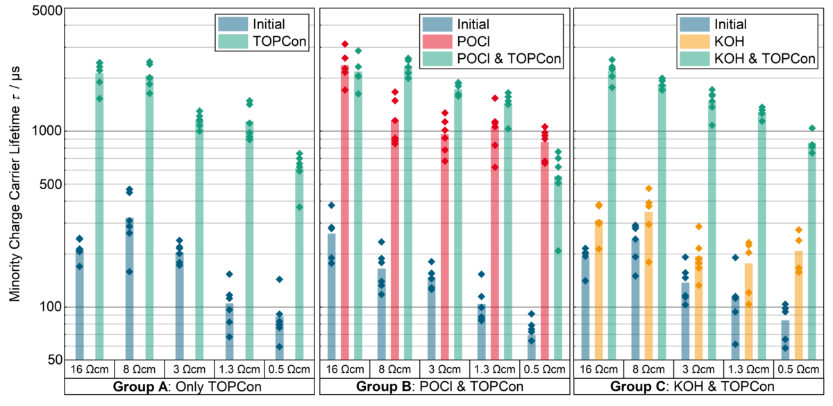
In the study, the researchers compared the gettering effect of the TOPCon layers to the established phosphorus gettering process. They systematically evaluated minority charge carrier lifetimes of n-type EpiWafers with base resistivities between 0.5 and 16 Ωcm.
Through this analysis, the research team found that for the 1.3 Ωcm EpiWafers, the average lifetimes increased from above 100 μs in the initial state to above 1 ms after TOPCon gettering and via the phosphorus gettering process. To evaluate the impact on cell performance parameters, the scientists used injection-dependent lifetime images for TOPCon bottom solar cell precursors with and without previous phosphorus gettering.
The results indicated that the standard base resistivity of 1 Ωcm and the parameters are comparable to those of float zone wafers and result in an estimated overall tandem device efficiency exceeding 30%. “This proves that the in situ gettering of TOPCon2 layers improves the material quality of EpiWafers sufficiently to fabricate perovskites silicon tandem solar cells with a high energy conversion efficiency and with low carbon footprint,” said the group.
The researchers used epitaxially grown silicon wafers similar to EpiWafers from German wafer manufacturer* NexWafe GmbH, a Fraunhofer ISE spinoff company. Rittmann explained that the proof-of-concept research at Fraunhofer ISE combined with NexWafe's industrial realization is “very exciting and promising.”
Their findings are available in the study “Effective in situ TOPCon Gettering of Epitaxially Grown Silicon Wafers during Bottom Solar Cell Fabrication,” published by Solar RRL.
Currently, the Fraunhofer ISE Center for High Efficiency Solar Cells (ZHS) is following up by fabricating bottom solar cells based on the research, according to Rittmann.
She also noted that the group known as Silicon Materials and Epitaxial Wafers, also at Fraunhofer ISE, is working on electrochemical etching and epitaxial growth of silicon wafers, as well as on germanium wafers for use in low-cost, reusable substrates for III-V tandem solar cell technologies.
*This article was corrected on 29 April 2025 to show that the epitaxially grown silicon wafers were grown by the researchers in the Fraunhofer ISE reactor.
Image: Fraunhofer ISE, Solar RLL, Creative Commons License CC BY 4.0
What's Your Reaction?