Gallium arsenide solar cells radiation-resilient for space applications
A group led by Cambridge University has developed an adhesive-free method of bonding ultra-thin gallium arsenide solar cells to borosilicate glass. The proposed technique is reportedly compatible with standard planar device processing.
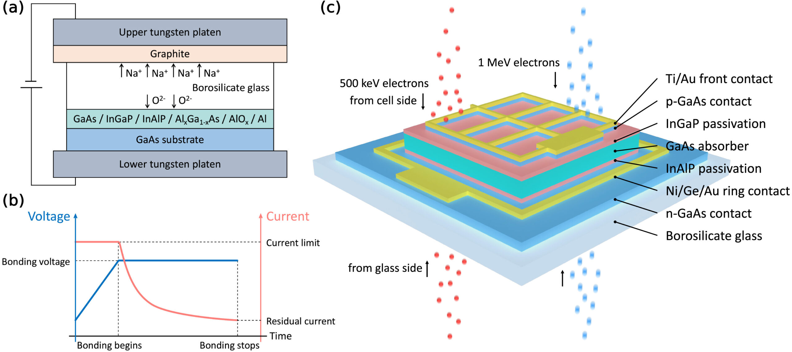
A group led by Cambridge University has developed an adhesive-free method of bonding ultra-thin gallium arsenide solar cells to borosilicate glass. The proposed technique is reportedly compatible with standard planar device processing.
A team of researchers led by the UK’s University of Cambridge has developed an adhesive-free method of bonding ultra-thin gallium arsenide (GaAs) solar cells to borosilicate glass. The technique, based on anodic bonding, offers higher specific power for radiation protection in space missions.
“Previous authors have demonstrated bonded thin solar cells with light management using adhesives; however, these materials are not fully compatible with standard planar device processing,” the team said. “Therefore, developing a method for bonding ultra-thin III-V solar cells to thermal expansion (CTE)-matched substrates is a key target for future applications of ultra-thin III-V solar cells in space.”
For the creation of their cell, the team began by growing GaAs layers using molecular beam epitaxy (MBE), followed by the removal of their native oxides. Placing it on borosilicate glass, the bonding process is initiated. It is performed in a bonding chamber, which is heated to up to 300 C, with a pressure of about 105 Pa. Under these conditions, a high voltage of up to 500 V is applied, causing the device to bond to the glass.
“The borosilicate glass used was D263 T eco from Schott, which has a CTE of 7.20×10⁻⁶ C−1, closely matched to that of GaAs at elevated bonding temperatures. It was found that this CTE matching was essential for strain management during bonding,” the researchers explained. “For initial attempts at GaAs anodic bonding, Borofloat 33 glass was used, which has a CTE mismatch to GaAs. This resulted in significant cracking as the bonded stack cooled to room temperature, despite the use of relatively low bonding temperatures minimizing thermal expansion.”
Image: University of Cambridge, Solar Energy Materials and Solar Cells, CC BY 4.0
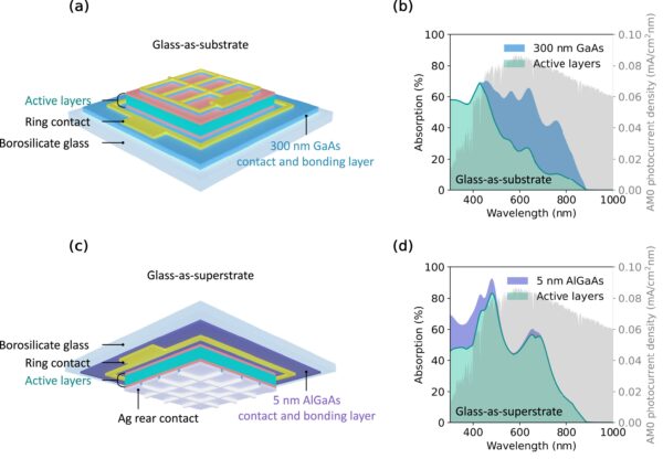
Following the completion of the bonding process, the growth wafer is removed by mechanical lapping and chemical etching. A titanium/gold layer was then thermally evaporated onto the p-type GaAs contact layer. In the area outside the mesa, a nickel-germanium-gold metal ring contact was deposited. This structure enables integrated light management for substrate, superstrate, or bi-facial orientations of the solar cells.
“In the glass-as-superstrate embodiment, the maximum power density (Pmax) remaining factor achieves 0.86 after 1 MeV electron exposure with a fluence of 3.6 × 1016 cm−2, equivalent to > 15 years in a geostationary orbit (GEO), exceeding that of current commercial triple-junction space solar cells,” the results showed. “The short-circuit current density (Jsc) of the ultra-thin GaAs solar cells with only 80 nm thick absorbers could be boosted to 17.69 mA/cm2 using higher bandgap III-V alloys as contact and bonding layers, with further improvement of integrating advanced light management approaches for higher power conversion efficiency.”
In addition, the researchers have emphasized that Pmax remaining factors for both substrate and superstrate orientations are higher than those of commercial triple-junction solar cells for space applications under 1 MeV electron irradiation.
Their findings were presented in “Radiation-resilient ultra-thin GaAs solar cells on glass transferred by anodic bonding,” published in Solar Energy Materials and Solar Cells. Researchers from the University of Cambridge in the United Kingdom, Japan’s National Institutes for Quantum Science and Technology (QST), Tohoku University, the Japan Aerospace Exploration Agency (JAXA), and Sanjo City University conducted the study.
What's Your Reaction?


