


High-temperature co-annealing step could cut TOPCon cell costs
Researchers at the Ecole Polytechnique Fédérale de Lausanne (EPFL) have proposed combining the two high-temperature steps used in producing tunnel oxide passivated contact (TOPCon) solar cells into a single co-annealing process. Initial results show promising outcomes in boron concentration, passivation quality, and contact resistivity.
Researchers at the Ecole Polytechnique Fédérale de Lausanne (EPFL) have proposed combining the two high-temperature steps used in producing tunnel oxide passivated contact (TOPCon) solar cells into a single co-annealing process. Initial results show promising outcomes in boron concentration, passivation quality, and contact resistivity.
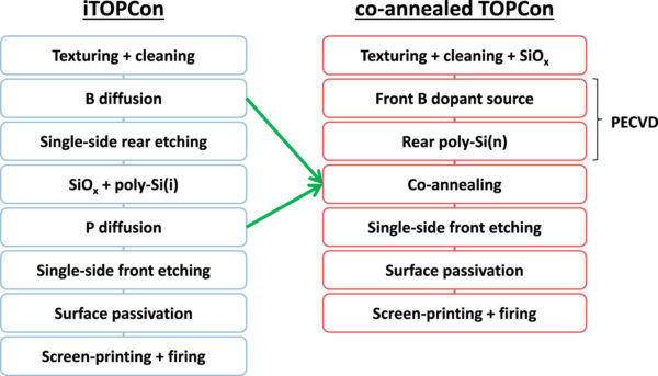
A research team led by Switzerland's EPFL has sought to simplify TOPCon solar cell production by combining the two required high-temperature steps – front-side emitter formation and rear passivating contact fabrication –into a single process.
The first process consists of depositing a borosilicate glass (BSG) layer in the cell, while the second step diffuses borosilicate from the BSG into the wafer.
“We investigated the front boron emitter formation process in greater depth, focusing on the co-annealing process,” researcher Thibault Schaller told pv magazine. “Building on the knowledge gained from previous experiments, we introduced a drive-in step in an oxygen environment into the co-annealing process, initially performed only in an air environment. With the introduction of this drive-in step, we succeeded in reducing recombination losses in the emitter and making it more compatible with standard industrial metallization approaches.”
Schaller said the rear passivating contact showed promising compatibility with the optimized co-annealing process. He added that the team aims to demonstrate proof-of-concept co-annealed TOPCon devices exceeding 24% efficiency in the lab, noting that the streamlined process could lower energy payback times and be especially beneficial in countries with high facility and equipment costs.
The proposed hybrid process is a “lean manufacturing” process for co-annealing, in which the front and rear doped layers are subsequently deposited by plasma-enhanced chemical vapor deposition (PECVD). Then, the co-annealing step is executed to form the front emitter and activate the rear passivating contact.
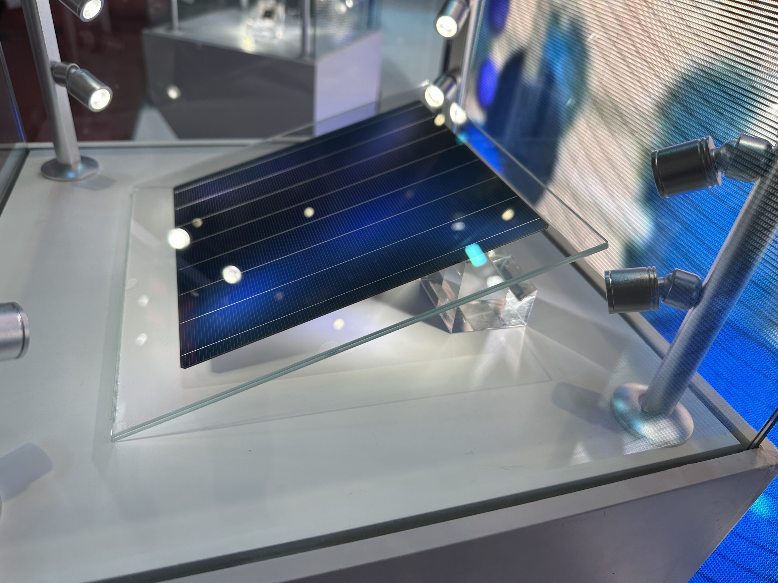
Image: EPFL, Solar Energy Materials and Solar Cells, CC BY 4.0
“Based on the knowledge acquired, we modify the co-annealing step by adding a drive-in phase carried out in an O2 environment in order to reduce the surface concentration and increase the emitter depth,” said the researchers.
A series of assessments and a feasibility analysis showed that the proposed two-step co-annealing process helps effectively reduce the surface concentration and increase the depth of emitters diffused from a plasma-deposited borosilicate diffusion source.
Through the single process, the academics achieved an emitter profile with a surface concentration of 2.2 × 1019 cm-3 and an emitter depth of 880 nm, which they said is fully compatible with standard industrial metallization obtained by screen-printing and firing-through silver (Ag) or aluminum (Al) metallization pastes.
However, the analysis also showed that the quality of the passivation after co-annealing was not uniform.
“We show that while this modification reduces the surface concentration and increases the emitter depth, resulting in reduced surface recombination and improved compatibility with standard industrial metallization processes,” the researchers also stated, noting that the new manufacturing technique is mostly intended to reduce TOPCon solar cell manufacturing costs.
Although the new process seems to offer good results in terms of boron concentration profile, passivation quality and contact resistivity, the scientists said further optimization is required.
The new manufacturing process was presented in the study “Boron-emitter development for TOPCon c-Si solar cells based on plasma-deposited boron diffusion source and poly-Si(n) passivating contact,” published in Solar Energy Materials and Solar Cells.
What's Your Reaction?